Author: Amirhossein Hajizadeh
Contact:
In electronic circuits, “biasing” refers to the application of dc voltages to establish a fixed level of current and voltage. This setup determines how much current flows and what voltage levels are present when there is no input signal. In the case of transistor amplifiers, the applied DC bias establishes a specific operating point on the device’s characteristic curves. This point defines the region of operation where the transistor will function properly for amplifying signals.
The operating point is also called the quiescent point (Q-point), which comes from the word quiescent, meaning still or inactive. It represents the steady-state condition of the circuit when no input signal is applied. Figure 2.1 illustrates a general device characteristic showing different possible operating points.
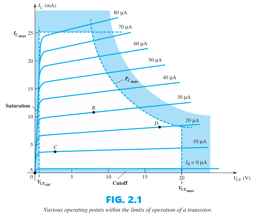
The biasing circuit can be designed to set the device’s operation at any of the indicated points or others within the active region. The maximum ratings are shown on the characteristics of Figure 2.1 by a horizontal line representing the maximum collector current $I_{C_{\text{max}}}$ and a vertical line representing the maximum collector-to-emitter voltage ($V_{CE_{\text{max}}}$). The maximum power constraint is specified by the curve $P_{C_{\text{max}}}$ in the same figure. At the lower end of the scales, the cutoff region is defined by $I_{B} ≤ 0 mA$, while the saturation region is defined by $V_{CE} ≤ V_{CE_{\text{sat}}}$. We can consider some differences among the various points shown in Fig. 2.1 to present some basic ideas about the operating point and, thereby, the bias circuit:
Load-line analysis finds the operating point by superimposing a device’s characteristic curves onto the straight-line equation produced by the surrounding network. The intersection of the two plots defined the actual operating conditions for the network. It is referred to as load-line analysis because the load (network resistors) of the network defined the slope of the straight line connecting the points defined by the network parameters. Just as this was true for a diode, the same approach can be applied to BJT networks. The characteristics of the BJT are superimposed on a plot of the network equation defined by the same axis parameters. The load resistor $R_{C}$ for the fixed-bias configuration will define the slope of the network equation and the resulting intersection between the two plots. The smaller the load resistance, the steeper the slope of the network load line. The network of Fig. 3.1a establishes an output equation that relates the variables $I_{C}$ and $V_{CE}$ in the following manner: \(V_{CE} = V_{CC}- I_{C}R_{C}~~~~(1)\)
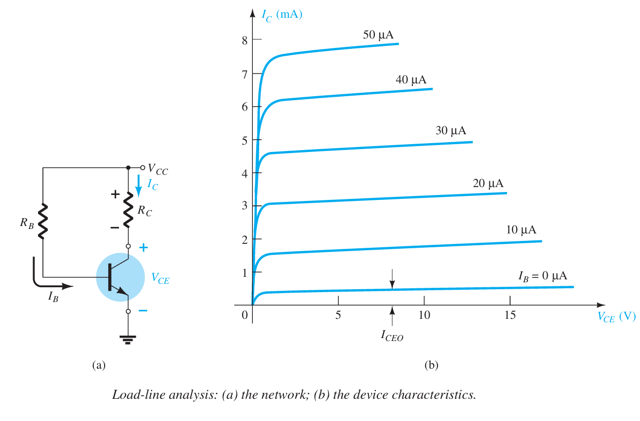
| The transistor’s output characteristics also relate the same two variables, $I_{C}$ and $V_{CE}$, as shown in Fig. 3.1b. The device curves of $I_{C}$ versus $V_{CE}$ are given in Fig. 3.1b. We now superimpose the straight line defined by Eq.(1) on these characteristics. The simplest way to plot Eq.(1) is to use two points, since a straight line is determined by two points. If we choose $I_{C} = 0 mA$, that point lies on the horizontal axis. Substituting $I_{C} = 0$ into Eq.(1) gives \(V_{CE} = V_{CC} - (0)R_{C}\), and $$V_{CE} = \left.V_{CC}\right | {I{C}=0~mA}~~~~(2)\(which defines one point on the line (see Fig. 3.2). If we choose $V_{CE} = 0v$, which lies on the vertical axis as the line on which the second point will be defined, we find that $I_{C}$ is determined by the following equation:\)0 = V_{CC} - I_{C}R_{C}\(and so\)I_{C} = \left.\frac{V_{CC}}{R_{C}}\right | {V{CE}=0~\mathrm{v}}~~~~(3)$$ This gives the second point on the line, as shown in Fig. 3.2. |
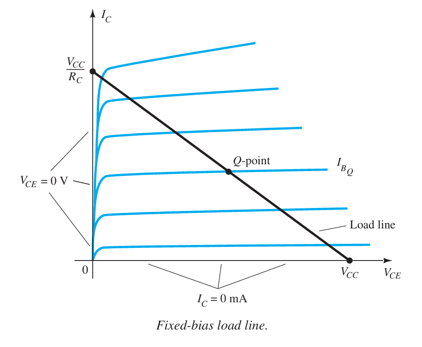
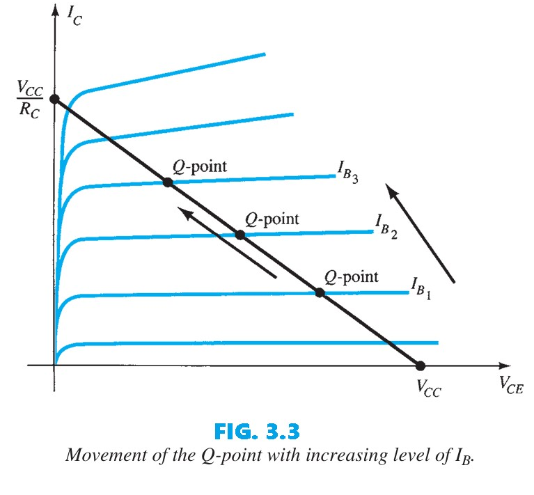
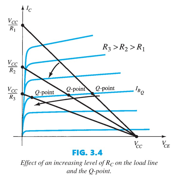
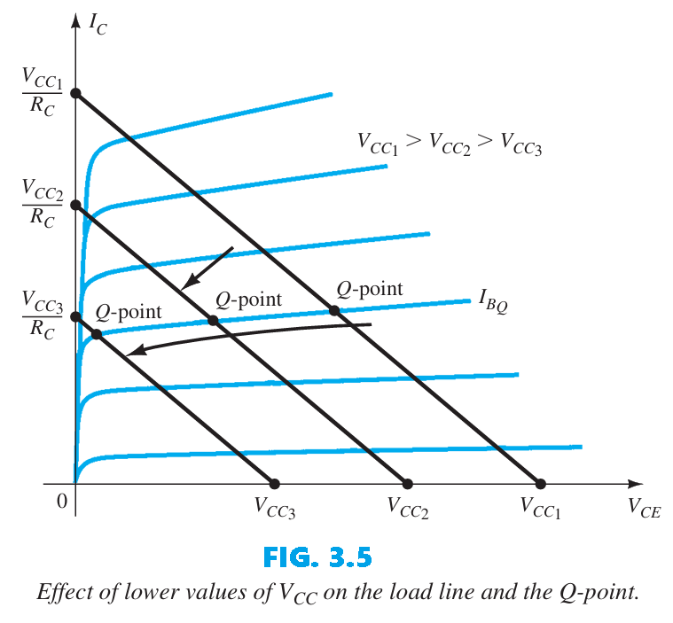
By joining the two points defined by Eqs. (2) and (3), we can draw the straight line established by Eq. (1). The resulting line on the graph of Fig. 3.2 is called the load line because it is defined by the load resistor $R_{C}$. By solving for the resulting level of $I_{B}$, we can establish the actual Q-point as shown in Fig. 3.2. If the level of $I_{B}$ is changed by varying the value of $R_{B}$, the Q-point moves up or down the load line as shown in Fig. 3.3 for increasing values of $I_{B}$. If $V_{CC}$ is held fixed and $R_{C}$ increased, the load line will shift as shown in Fig. 3.4. If $I_{B}$ is held fixed, the Q-point will move as shown in the same figure. If $R_{C}$ is fixed and $V_{CC}$ decreased, the load line shifts as shown in Fig. 3.5.
The circuit in Fig. 4.1 represents the simplest diode configuration. It is used to demonstrate how to analyze a diode circuit based on its actual characteristics. Later, the characteristics will be replaced by an approximate diode model to allow comparison of the results. Solving the circuit of Fig. 4.1 is all about finding the current and voltage levels that will satisfy both the characteristics of the diode and the chosen network parameters at the same time.
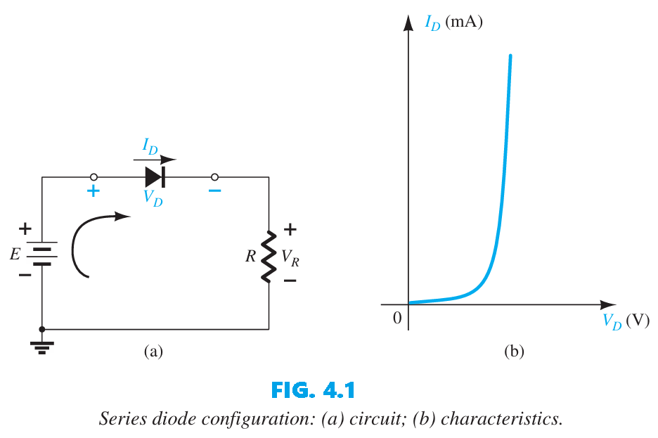
In Fig. 4.2 the diode characteristic is plotted together with a straight “load line” set by the network (its vertical intercept determined by the applied load $R$), and the intersection of the two curves gives the circuit solution — the voltage and current levels. To anticipate that solution for the simple circuit of Fig. 4.1, note that the DC source drives a clockwise conventional current which aligns with the diode symbol, so the diode is forward-biased and conducting; the polarities of $V_{D}$ and the direction of $I_{D}$ confirm this, giving a diode voltage near 0.7 V and a current on the order of 10 mA or more.
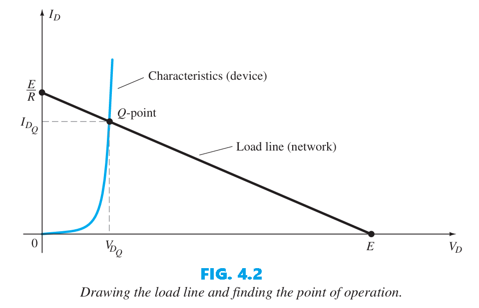
To find where the load line intersects the diode characteristics in Fig. 4.2, apply Kirchhoff’s voltage law around the loop in the clockwise direction to obtain \(+E- V_{D}- V_{R} = 0\) or \(E = V_{D} + I_{D}R~~~~(4)\)
| The two variables in Eq. (4), $V_{D}$ and $I_{D}$, are the same as the diode-axis variables in Fig. 4.2, which allows Eq. (4) to be plotted on the same characteristics shown in Fig. 4.2. The intersections of the load line and the characteristics can be found by using the fact that any point on the horizontal axis corresponds to $I_{D}$ and any point on the vertical axis corresponds to $V_{D}$. If we set $V_{D} = 0 v$ and substitute into Eq. (4), then solve for $I_{D}$, we obtain the magnitude of $I_{D}$ on the vertical axis. Therefore, with $V_{D} = 0 v$, Eq. (4) becomes \(E = V_{D} + I_{D}R\) \(= 0 v + I_{D}R\) and $$I_{D} = \left.\frac{E}{R}\right | {V{D}=0 ~\mathrm{v}}~~~~(5)$$ |
| as shown in Fig. 4.2. If we set $I_{D} = 0 A$ in Eq. (4) and solve for $V_{D}$, we have the magnitude of $V_{D}$ on the horizontal axis. Therefore, with $I_{D} = 0 A$, Eq. (4) becomes \(E = V_{D} + I_{D}R\) \(= V_{D} + (0 A)R\) and $$V_{D} = \left.\{E}\right | {I{D}=0 ~\mathrm{A}}~~~~(6)$$ |
as shown in Fig. 4.2. A straight line drawn between the two points will define the load line. Change the level of R (the load) and the intersection on the vertical axis will change. The result will be a change in the slope of the load line and a different point of intersection between the load line and the device characteristics. We now have a load line defined by the network and a characteristic curve defined by the device. The point of intersection between the two is the point of operation for this circuit. By simply drawing a line down to the horizontal axis, we can determine the diode voltage $V_{D_{Q}}$, whereas a horizontal line from the point of intersection to the vertical axis will provide the level of $I_{D_{Q}}$. The current $I_{D}$ is actually the current through the entire series configuration of Fig. 4.1a. The point of operation or the operating point is usually called the quiescent point (abbreviated “ Q point”). The solution obtained at the intersection of the two curves is the same as would be obtained by a simultaneous mathematical solution of \(I_{D} = \frac{E}{R} - \frac{V_{D}}{R}~~~~ [derived~from~Eq.~(4.1)]\) and \(I_{D} = I_{S}(e^{\frac{V_{D}}{nV_{T}}} - 1)\)
The load-line analysis described above provides a solution with minimum effort and offers a visual explanation of why the $V_{D_{Q}}$ and $I_{D_{Q}}$ levels were obtained.
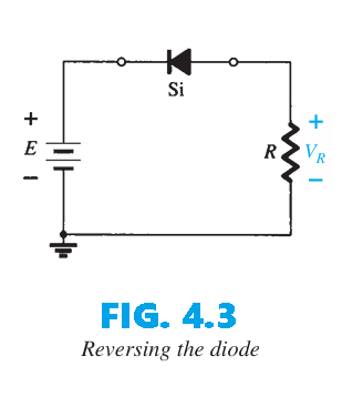
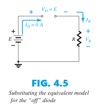
We now consider the diode in the reverse-biased configuration. Mentally replacing the diode with a resistive element, as depicted in Fig. 2.11, reveals that the resulting current direction does not match the arrow on the diode symbol. Consequently, the diode is in the “off” state, yielding the equivalent circuit of Fig. 2.12. Since the circuit is open, the diode current is $0 A$ and the voltage across the resistor $R$ is the following: \(V_R=I_RR=I_DR=(0~A)R=\bold{0~V}\)
The diode analysis will now be extended to cover time-varying functions such as the sinusoidal waveform and the square wave. Once a few fundamental techniques are understood, the analysis becomes fairly direct and follows a common thread. Figure 5.1 shows the simplest network to examine with a time-varying signal. For the moment, we adopt the ideal model to ensure the approach is not obscured by additional mathematical complexity.
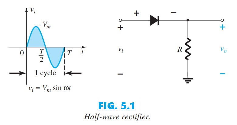
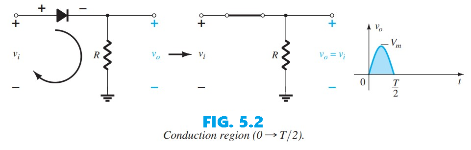
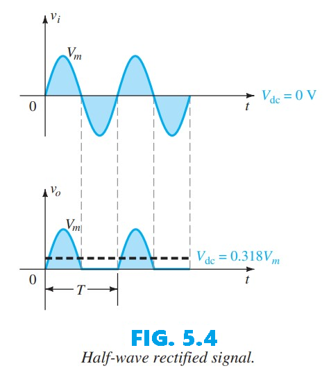
Over one full cycle (the period ($T$) in Fig. 5.1) the average value—the algebraic sum of the areas above and below the axis—is zero. The circuit of Fig. 5.1, called a half-wave rectifier, produces an output waveform $v_o$ whose average value is of particular use in the ac-to-dc conversion process. When employed for rectification a diode is typically referred to as a rectifier and therefore has power and current ratings much higher than those of diodes used in other applications, such as computers and communication systems. During the interval ($t = 0 \rightarrow \frac{T}{2}$) in Fig. 5.1 the polarity of the applied voltage $v_i$ establishes a “pressure” in the indicated direction that turns the diode on, with the polarity appearing above the diode. Substituting the short-circuit equivalence for the ideal diode gives the equivalent circuit of Fig. 5.2, where it is clear that the output signal is an exact replica of the applied signal because the two terminals defining the output voltage are connected directly to the applied signal via the diode’s short-circuit equivalence.
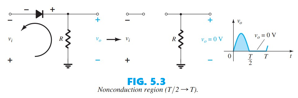
Over the period $\frac{T}{2} \rightarrow T$, the polarity of the input $v_i$ (shown in Fig. 5.3) causes the polarity across the ideal diode to place it in the “off” state, producing an open-circuit equivalent. Consequently, there is no path for charge to flow, and $v_o = iR = (0)R = 0\ \text{V}$ for the period $\frac{T}{2} \rightarrow T$. For comparison, the input $v_i$ and the output $v_o$ are sketched together in Fig. 5.4.
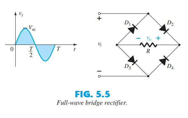
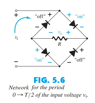
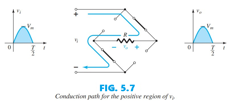
The DC level obtained from a sinusoidal input can be increased by 100% using a process called full-wave rectification. The most familiar network for this function is shown in Fig. 5.5, with its four diodes arranged in a bridge configuration. During the period $t = 0$ to $T/2$ the polarity of the input is as shown in Fig. 5.6. The resulting polarities across the ideal diodes, also shown in Fig. 5.6, indicate that $D_2$ and $D_3$ conduct whereas $D_1$ and $D_4$ remain in the “off” state. The net result is the configuration of Fig. 5.7, with the indicated current and polarity across $R$. Because the diodes are ideal, the load voltage is $v_o = v_i$, as illustrated in the same figure.
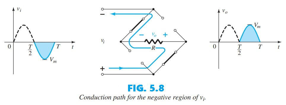
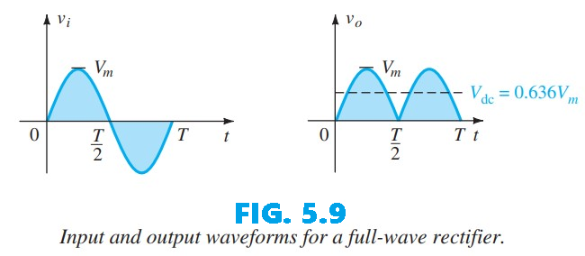
During the negative half-cycle of the input, diodes $D_1$ and $D_4$ conduct, producing the configuration shown in Fig. 5.8. The key result is that the polarity across the load resistor $R$ remains the same as in Fig. 5.6, creating a second positive pulse, as illustrated in Fig. 5.8. Over one complete cycle, the input and output voltages appear as shown in Fig. 5.9.
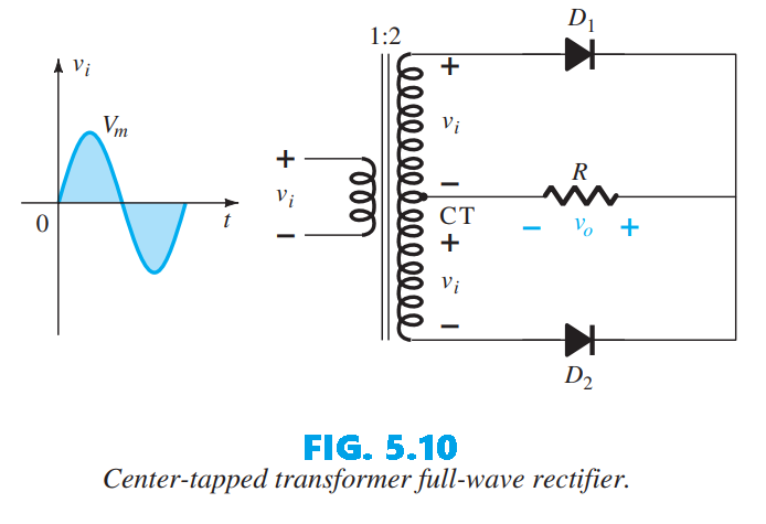
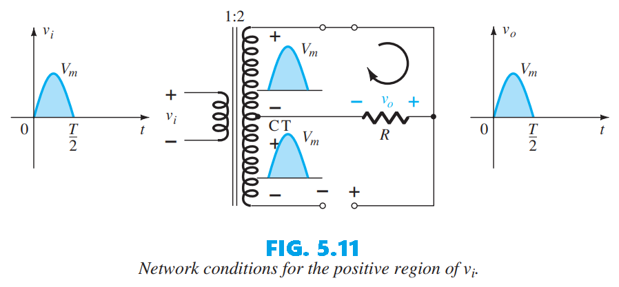
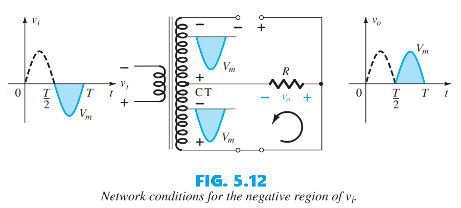
A second common full-wave rectifier, shown in Fig. 5.10, uses only two diodes but requires a center-tapped transformer so each half of the secondary of the transformer supplies the input during alternating half-cycles. In the positive portion the circuit looks like Fig. 5.11: each half of the secondary produces a positive pulse, D1 conducts (behaves like a short) and D2 is off (behaves like an open) according to the secondary voltages and current directions; the resulting output is shown in Fig. 5.11.
During the negative half-cycle, the circuit appears as in Fig. 5.12 and the diodes swap roles, yet the voltage across the load R retains the same polarity. The overall output and DC level are therefore the same as those in Fig. 5.9.
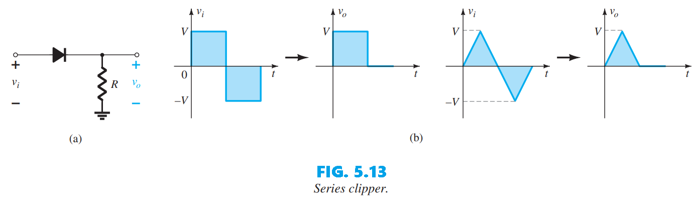
Clippers are another form of diode-based circuits that change the appearance of an applied waveform. They are networks that employ diodes to “clip” away a portion of an input signal without distorting the remaining part of the waveform. There are two general categories of clippers: series and parallel. The series configuration is defined as one where the diode is in series with the load, whereas the parallel variety has the diode in a branch parallel to the load. Figure 5.13b illustrates how the series clipper of Fig. 5.13a responds to a range of alternating waveforms. Although it was originally presented as a half-wave rectifier for sinusoids, the circuit will clip virtually any input waveform.
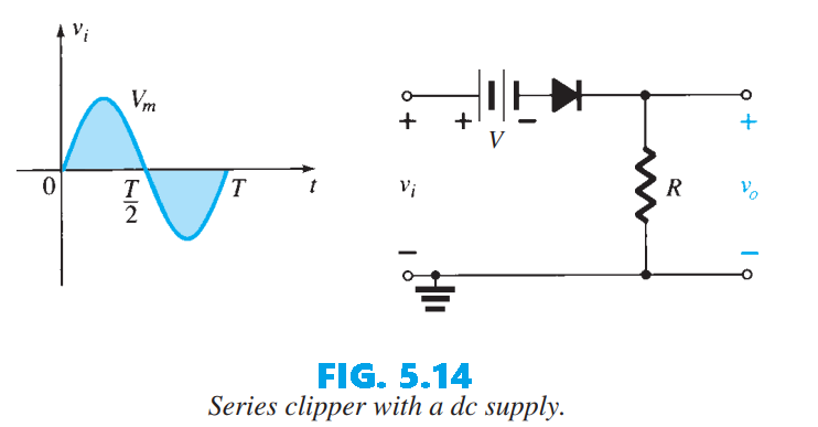
Adding a DC source (see Fig. 5.14) significantly alters the behavior and complicates the analysis: the DC bias can either reinforce or oppose the AC source and may be placed in series between the supply and output or in a branch parallel to the output, with each arrangement producing different clipping outcomes.
There are some important steps one can take to give the analysis some direction. Here are some of them: 1) Note precisely where the output voltage is measured. 2) Build an intuitive picture of the circuit by identifying the voltage (or “pressure”) each source produces and how that drives conventional current through the diode. 3) Find the transition voltage at which the diode changes state — the input level that switches it from off to on. 4) When sketching results, plot the output waveform directly beneath the input using the same horizontal and vertical scales to make comparisons straightforward.
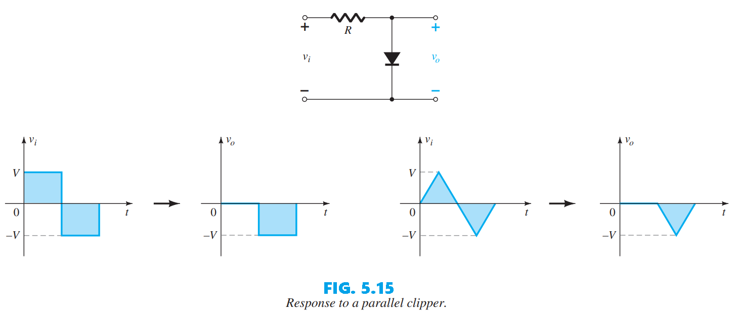
For the parallel section we consider the network of Fig. 5.15, the simplest parallel diode arrangement subjected to the input signals of Fig. 5.13. The analytical approach closely mirrors that used for series clippers.
In the previous part, several diode configurations were analyzed that removed specific portions of the input signal while leaving the rest of the waveform unchanged. Here, we will explore various diode arrangements that instead shift the entire input signal to a different voltage level. A clamper is a network constructed of a diode, a resistor, and a capacitor that shifts a waveform to a different dc level without changing the appearance of the applied signal.
By adding a DC supply to the basic clamper, the output can be shifted by additional amounts. The resistor and capacitor should be chosen so that the time constant $\tau=RC$ is large enough that the capacitor’s voltage does not appreciably discharge while the diode is nonconducting; for practical purposes we take a capacitor to be fully charged or discharged after about five time constants.
The simplest clamper (Fig. 5.16) places the capacitor directly between the input and output, while the resistor and diode appear in parallel with the output. In many clamping circuits the diode may also include a series DC source to produce a further offset.
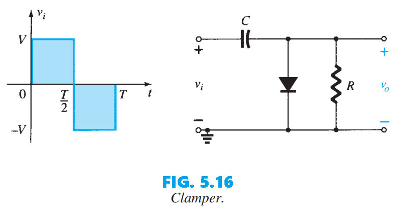
There is a sequence of steps that can be applied to help make the analysis straightforward: 1) Begin by looking at the part of the input waveform that makes the diode conduct (i.e., the interval that forward-biases the diode). 2) While the diode is conducting, treat the capacitor as if it charges instantly to the voltage set by the surrounding circuit. 3) When the diode is nonconducting, assume the capacitor preserves the voltage it acquired (it does not change appreciably). 4) Always keep track of the output node $v_o$—its location and polarity—so the voltage levels are interpreted correctly. 5) Confirm that the output’s total voltage excursion equals the input’s total swing.
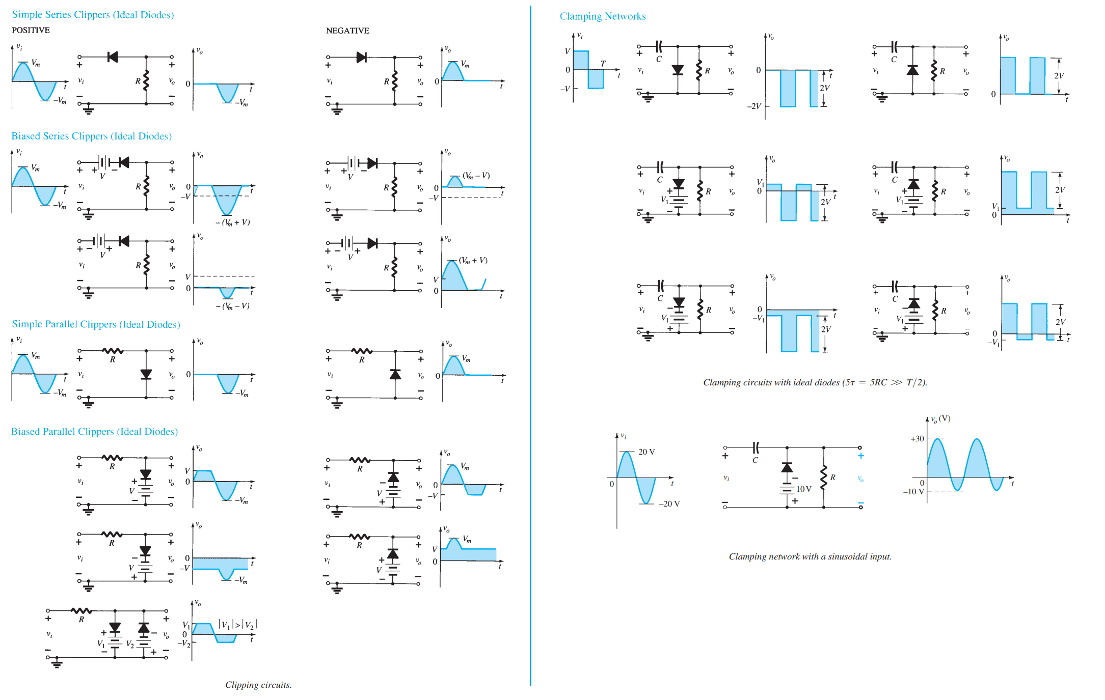
A number of clipping and clamping circuits and their effect on the input signal are shown in Fig. 5.17 below:
Temperature affects a diode’s operation point by decreasing the forward voltage drop, which causes the forward current to increase for a given voltage, and by significantly increasing the reverse saturation current. For silicon diodes, the forward voltage decreases by about $2.5 mV$ per degree Celsius increase, while the reverse saturation current doubles for every $10^\circ C$ rise in temperature.
Effects on forward bias:
Effects on reverse bias:
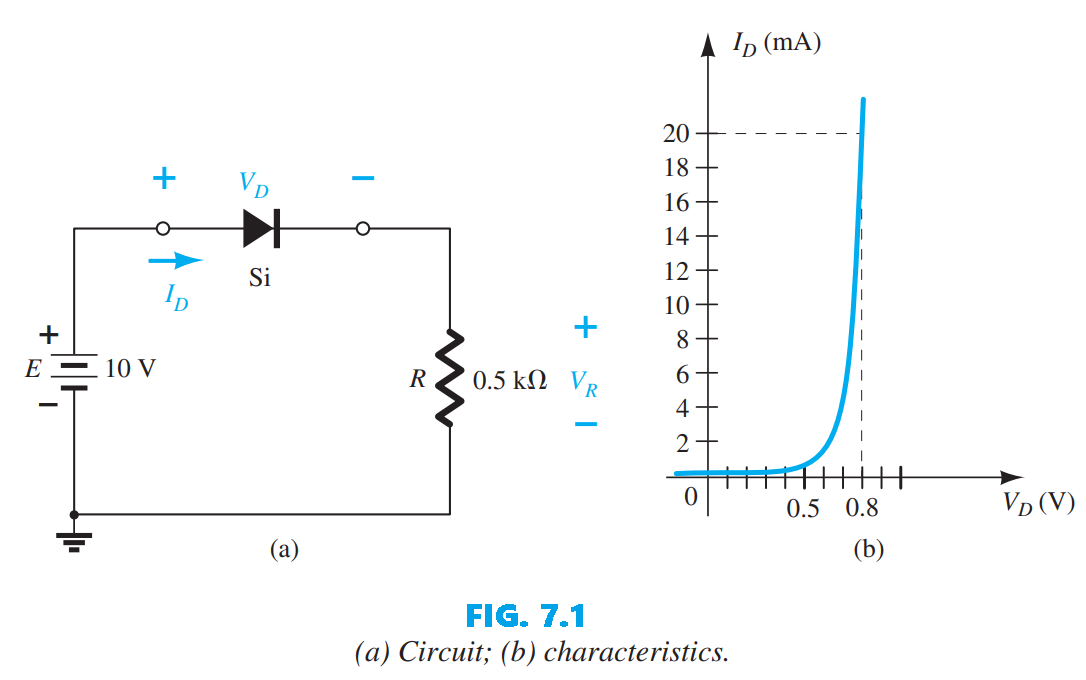
Example 1: For the series diode configuration of Fig. 7.1a , employing the diode characteristics of Fig. 7.1b , determine: a. $V_{D_{Q}}$ and $I_{D_{Q}}$ b. $V_R$
Solution:
a. Eq (5): $I_{D} = \left.\frac{E}{R}\right|{V{D}=0 ~\mathrm{V}}=\frac{10V}{0.5k\Omega}=20mA$
Eq (6): $V_{D} = \left.\{E}\right|{I{D}=0 ~\mathrm{A}}=10V$
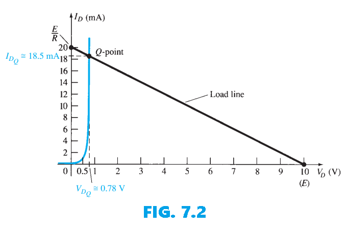
After plotting these points on the x axis and the y axis, the resulting load line appears in Fig. 7.2 . The intersection between the load line and the characteristic curve defines the Q-point as \(V_{D_{Q}}≅0.78V\) \(I_{D_{Q}}≅18.5mA\)
The level of $V_D$ is certainly an estimate, and the accuracy of $I_D$ is limited by the chosen scale. A higher degree of accuracy would require a plot that would be much larger and perhaps unwieldy. b. $V_R=E-V_D=10V-0.78V=9.22V$
As noted in this example, the load line is determined solely by the applied network, whereas the characteristics are defined by the chosen device. Since the network of Example 7.1 is a dc network the Q-point of Fig.7.2 will remain fixed with $V_{DQ} = 0.78 V$ and $I_{DQ} = 18.5 mA$. By Ohm’s law we know that a dc resistance is defined at any point on the characteristics by $R_{DC} = \frac{V_D}{I_D}$.
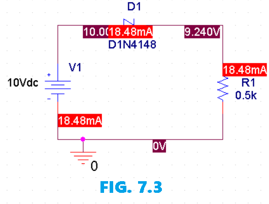
After running a bias-point (operating-point) analysis on the same circuit in PSpice, the diode’s operating values were directly read from the operating point report. The simulated diodevoltage $V_D$ and the diode current $I_D$ were found with the expected/reference values from the original solution as shown in Fig. 7.3:
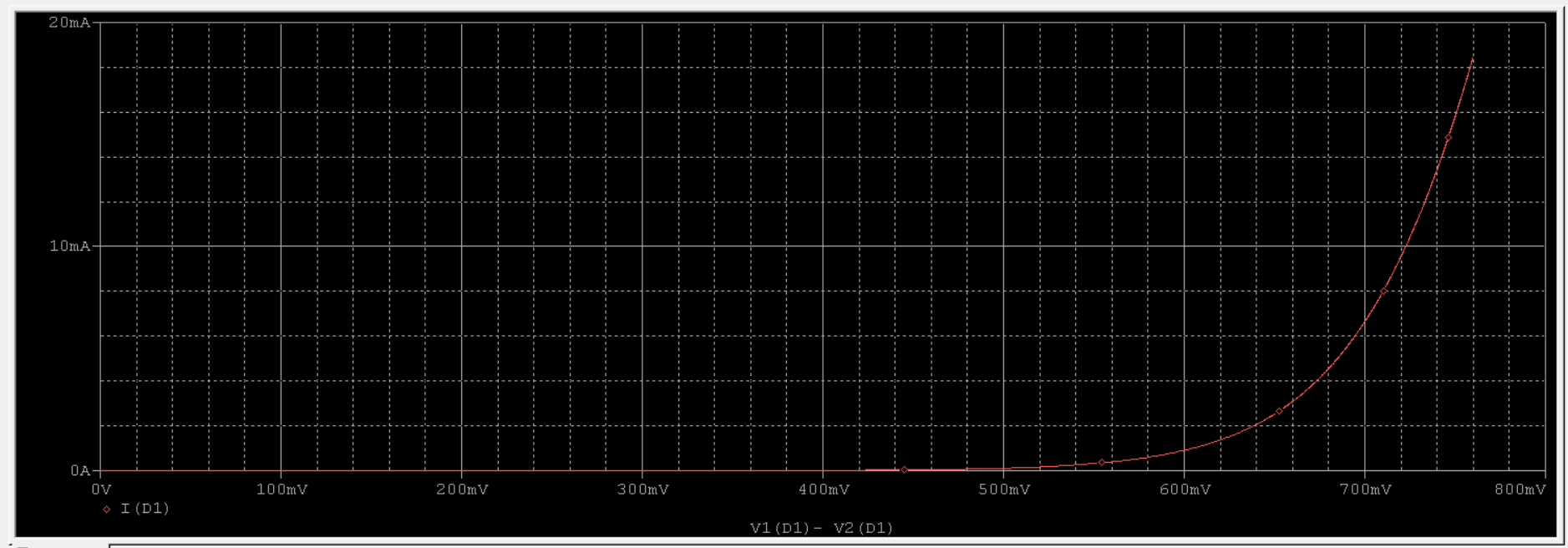
Next, a DC Sweep analysis of the source were performed and plotted the diode characterestics (diode voltage on the x_axis and diode current on the y_axis). As shown in Fig. 7.4, We can see that the diagram matches the original one from the example.
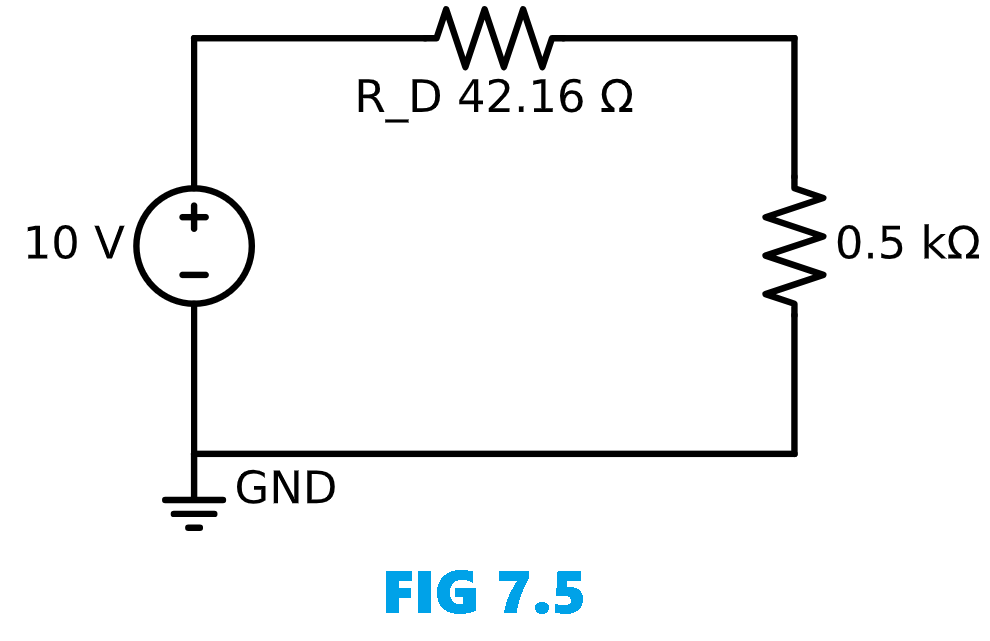
Using the Q-point values, the dc resistance for Example 1 is \(R_D=\frac{V_{D_{Q}}}{I_{D_{Q}}}=\frac{0.78V}{18.5mA}=42.16\Omega\) An equivalent network (for these operating conditions only) can then be drawn as shown in Fig. 7.5:
Example 2: Determine $v_o$ for the network of Fig. 7.6:
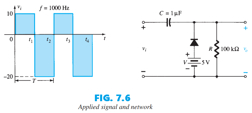
Solution:
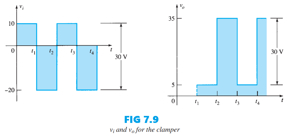
At $f=1kHz$ the period is $1 ms$, so each level lasts $0.5 ms$. Let’s start the analysis with the period $t_1 \rightarrow t_2$, during which the diode is effectively int short-circuit state. In this interval the circuit reduces to the form drawn in Fig. 7.7. Because the defined terminals for $v_o$ are the same nodes as the 5-V source, the output appears directly across the battery and across $R$; therefore $v_o = 5V$ for this interval. Applying Kirchhoff’s voltage law around the input loop then yields:
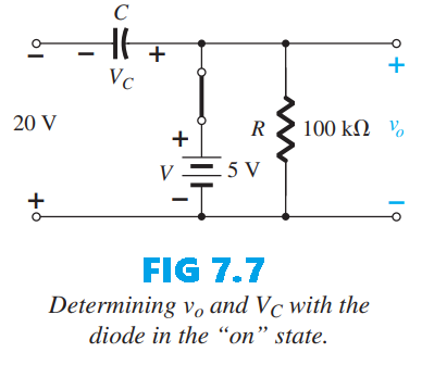
\(-20 V + V_C - 5 V = 0\) and \(V_C = 25 V\)
The capacitor will therefore charge up to $25 V$. In this case the resistor $R$ is not shorted out by the diode, but a Thévenin equivalent circuit of that portion of the network that includes the battery and the resistor will result in $R_{Th} = 0$ with $E_{Th} = V = 5 V$. For the period $t_2 \rightarrow t3$ the network will appear as shown in Fig. 7.8. The open-circuit equivalent for the diode removes the 5-V battery from having any effect on $v_o$, and applying Kirchhoff’s voltage law around the outside loop of the network results in \(+10 V + 25 V - v_o = 0\) and \(v_o = 35 V\)
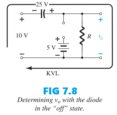
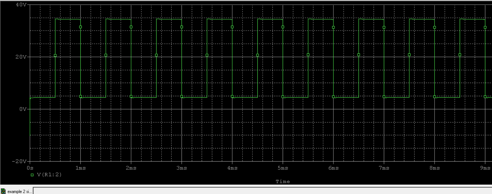
The time constant of the discharge network shown in Fig. 7.8 is given by the product $\tau = RC$. Using the stated values, \(\tau = RC = 100k\Omega \times 1 \times 10^{-7} = 1 \times 10^{-2} s = 10 ms\) The total discharge interval, taken as $5\tau = 5(10ms) = 50ms$. Because the interval $t_2 \rightarrow t_3$ lasts only $0.5 ms$, it is an excellent approximation to treat the capacitor voltage as essentially constant during the brief discharge between input pulses. The resulting steady output, plotted together with the input in Fig. 7.9, exhibits an output swing of $30V$, which corresponds to the input swing as noted previously.
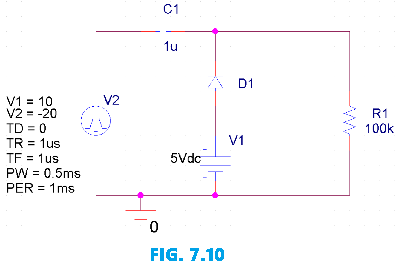
For simulation purposes this circuit was designed in OrCAD Capture exactly as described—an input PULSE source configured to alternate between +10 V and −20 V at 1 kHz (period = 1 ms), a 1-µF coupling capacitor from the source to the output node, a 5-V DC source with a diode in series tied to that node, and a 100-kΩ resistor from the node to ground— (circuit shown as Fig. 7.10), then created a transient simulation profile (run time long enough to reach steady periodic behavior, e.g. 10 ms, with a small maximum time step such as 1 µs) and generated the netlist. The transient analysis was then ran, opened the PSpice A/D Probe waveform viewer, and added the trace $v_o$ to observe the output; the plotted waveform is shown as Fig. 7.11. As you can see the simulation matches the $v_o$ defined in the solution.